printed circuit board
[′print·əd ′sər·kət ‚bȯrd]printed circuit board
(hardware)The simplest kind of PCB has components and wires on one side and interconnections (the printed circuit) on the other. PCBs may have components mounted on both sides and may have many internal layers, allowing more connections to fit in the same board area. Boards with internal conductor layers usually have "plated-through holes" to improve the electrical connection to the internal layers.
The connections are metal strips (usually copper). The pattern of connections is often produced using photo-resist and acid etching. Boards, especially those for high frequency circuits such as modern microprocessors, usually have one or more "ground planes" and "power planes" which are large areas of copper for greater current carrying ability.
A computer or other electronic system might be built from several PCBs, e.g. processor, memory, graphics controller, disk controller etc. These boards might all plug into a motherboard or backplane or be connected by a ribbon cable.
printed circuit board
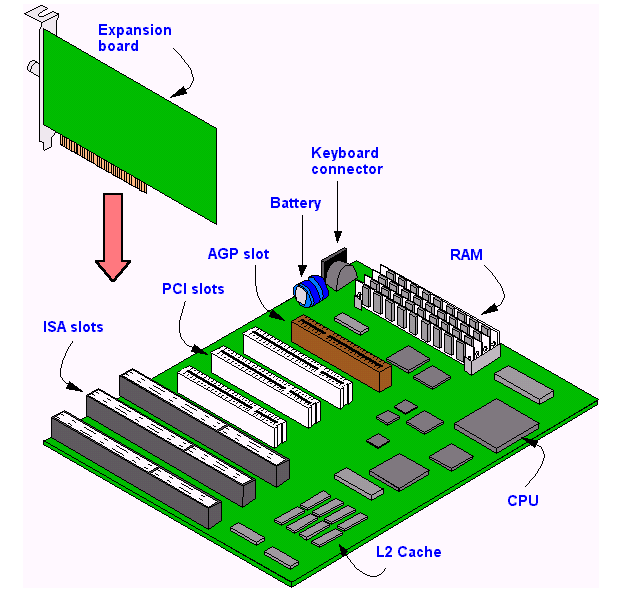
A rigid, flat board that holds chips and other electronic components. The printed circuit board (PCB) is made of layers, from two to a dozen or more, that interconnect components via copper pathways. The main board in a computer is called the "system board" or "motherboard," while smaller ones that plug into slots on the main board are called "boards" or "cards." See motherboard, expansion card and flexible circuit.Etched Circuits
The "printed" circuit is an etched circuit. A copper foil is placed over a fiberglass or plastic base of each layer and covered with a photoresist. Light is beamed through a negative image of the circuit paths onto the photoresist, hardening the areas that will remain after etching. When passed through an acid bath, the unhardened areas are washed away, and the finished layers are then glued together. The etching process is also used to create integrated circuits (chips).
Starting in the 1940s
Printed circuit boards (PCBs) were first used in the 1940s to connect discrete components together. By the 1960s, they were widely used in all electronic systems, and as integrated circuits emerged in the 1970s, chips were increasingly mounted on the boards. Today, PCBs hold a few discrete elements but mostly chips, and each chip contains from thousands to billions of transistors (see chip). See surface mount, via and discrete component.
 |
| Motherboard and Expansion Cards |
|---|
| This Baby AT board is an example of an early PC motherboard. It accepted both ISA and PCI cards containing peripheral controllers. See ISA and PCI. |
 |
| Boards Can Be Very Small |
|---|
| This earlier WOW HD board from SRS Labs created a more dynamic music experience. The complex processing that takes place on tiny PCBs such as this was unthinkable in the early days of computing. (Images courtesy of SRS Labs, Inc.) |
Printed Circuit Board
a board whose surfaces have printed current conductors with contact areas, which are used to connect components mounted on the boards according to the circuit diagram of a functional subassembly for electric or radio apparatus, and also have plated circuit holes and nonplated mounting holes. There are about 200 methods for making printed circuit boards; among the most important are the photochemical, photoelectrochemical, and offset-electrochemical methods. The methods differ in the means of producing the conductive coating or the form in which the pattern of the printed conductors is realized.
The dimensions of printed circuit boards, the position of the hole centers, and the hole diameters are standardized. The boards are 10–360 mm long, 10–240 mm wide, and 0.05–3.0 mm thick (depending on the rigidity required). The spacing of the coordinate grid for marking the holes is 2.5 mm or, less frequently, 1.25 mm, and the hole diameters range from 0.2 to 3 mm. A distinction is made among one-sided, two-sided, and multilayer boards (up to 15 layers). Multilayer boards are made by using extended leads, by metallizing the walls of through holes, by molding two-sided boards in pairs, or by layer-by-layer buildup. The material most often used for printed circuit boards are metal-clad and plain Micarta and fiberglass laminates, reinforced fluorine plastic, polystyrene, polyethylene terephthalate, polyamide, polycarbonate, and radioceramics.
REFERENCE
Konstruirovanie i tekhnologiia pechatnykh plat. Moscow, 1973.B. P. LIKHOVETSKII